
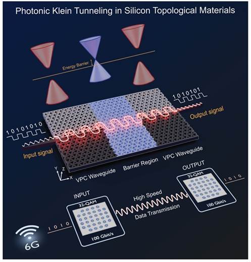
Scientists in India have developed a silicon-based microchip capable of guiding terahertz radiation past structural obstructions with minimal signal degradation, achieving data transfer rates of up to 100 gigabits per second. The innovation, engineered by a team at the Jawaharlal Nehru Centre for Advanced Scientific Research (JNCASR), overcomes a major hurdle in designing compact circuitry for upcoming sixth-generation (6G) cellular networks.
Wireless systems operating in the terahertz spectrum—situated between microwave frequencies and infrared light—offer vast bandwidth potential. However, traditional waveguides frequently suffer from heavy signal reflection and scattering when encountering structural joints, sharp corners, or internal barriers within microchips.
To counter signal loss, the research team applied topological photonics to build a photonic crystal on high-resistivity silicon, a material compatible with standard semiconductor fabrication lines. By arranging triangular perforations in a honeycomb lattice patterned after graphene, the microchip forces terahertz signals along designated boundary paths. Even when deliberate topological barriers were introduced by modifying hole dimensions, signal attenuation remained capped at 1–2 percent for a single barrier and 2–3 percent for two sequential barriers.
During high-speed transmission experiments operating between 310 and 360 GHz, a power splitter configuration utilizing 32-QAM modulation achieved 100 gigabits per second. At this speed, a standard 5-gigabyte high-definition video file can transfer in under half a second. Alternative test geometries, including an omega-shaped path featuring four right-angle turns and a central barrier, maintained throughput speeds of 60 gigabits per second.
The project was led by Dr. Abhishek Kumar, Assistant Professor at JNCASR and head of the Meta-Optics Laboratory, alongside joint lead authors Samina Mulla and Sangram Kumar Sadhu. The effort included collaborators from IISER Kolkata, IIT Bombay, A*STAR Singapore, and France’s CNRS and University of Lille.
“Demonstrating that terahertz waves can penetrate a barrier created by simply changing the geometry of the holes and still carry data at speeds of 100 gigabits per second suggests that this effect could become a useful design tool for terahertz chips,” said Dr. Abhishek Kumar.
Moving forward, the research team aims to integrate active electrical, thermal, or mechanical impedance controls to dynamically reroute signals across microchip pathways. The complete findings have been published in the journal Advanced Materials.
This report is based on official news releases issued by the Press Information Bureau (PIB), Delhi.